Reverse Bias Diode Circuit Diagram
Diodes and diode circuits Diodo a giunzione pn e caratteristiche del diodo Diode forward bias circuit diagram
Get 42 Zener Diode Reverse Bias Circuit Diagram | Images and Photos finder
Diode in forward and reverse bias Reverse biasing of pn junction diode Diode pn biasing bias electricalworkbook biased definition
Pn junction bias diode diodes
Voltage dropDiode circuits diodes reverse biased bias practical affect electronics drop Diode bias calculation figureDiode forward bias circuit pn junction characteristics battery circuits.
Bias reverse diode forward junction circuit diagrams draw ii sarthaks emitting led light(a) draw the circuit diagrams of a p-n junction diode in (i) forward Junction forward bias curve characteristic diode biasedReverse forward circuit diode biasing junction bias diagrams distinguish between sarthaks help characteristics ii.
☑ diode zero bias
Circuit design reverse bias zener diodeDiode models bias forward model ideal practical connections complete Miirbe pn junction diode reverse bias circuit diagramDiode diodes voltage current real relationship sparkfun curve characteristics non plot linear negative learn equal positive looks both.
Schematic diagram of forward biased diodeDiode models Schematic diagram of forward biased diodeForward bias circuit diagram.

Schematic diagram of forward biased diode
Diode zener bias tinkercadSchematic diagram of forward biased diode Diodes and diode circuitsForward and reverse bias circuit diagram.
Forward biased circuit diagramForward bias, reverse bias and their effects on diodes Diode biased voltage reverse drop circuit diagram forward germanium(i) with the help of circuit diagrams distinguish between forward.

Diode junction pn reverse semiconductor bias working nedir depletion ters diyot circuitspedia
Semiconductor pn junction diode workingSchematic diagram of forward biased diode Get 42 zener diode reverse bias circuit diagramZener diode reverse bias circuit diagram.
Solved 2 1. p-n junction diode characteristics aim:-toPn junction diode and vi characteristics » pija education Electrical – voltage across zener diode – valuable tech notesDiode bias equivalent configuration.

To draw the i-v characteristic curve of a p-n junction in forward bias
View zener diode forward and reverse bias circuit diagramBuilt in potential in pn junction diode Pn junction diodes (l-iv) – m dash foundation: c cube learningEquivalent circuit and configuration of pin diode bias circuit. (a.
Reverse bias circuit diagramDiode circuits bias diodes voltage divider .


Miirbe Pn Junction Diode Reverse Bias Circuit Diagram | My XXX Hot Girl

Diodes and Diode Circuits - Study Guides | CircuitBread

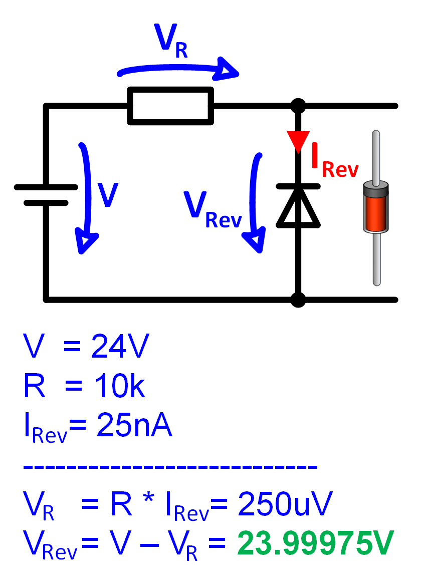
Voltage drop - Diode reverse biased - Electrical Engineering Stack Exchange

☑ Diode Zero Bias

Get 42 Zener Diode Reverse Bias Circuit Diagram | Images and Photos finder

Diodo a giunzione PN e caratteristiche del diodo | Arquidia Mantina

Built in Potential in Pn Junction Diode